As the term implies, reverse engineering (RE) is the act of taking apart an engineered or designed product or device back to its elemental engineering/design components. The motivation for such an act may be varied anywhere from competitive analysis and patent infringement detection to legacy design recovery. Nevertheless, they all include the need/desire to understand how the product/device was built/designed. The word “how” is used in its broadest sense here, including the questions of “what was used to build it,” “where each element fits,” “when certain events take place,” etc.
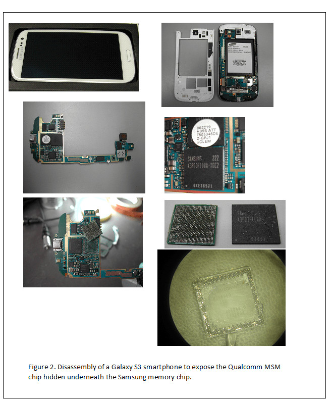
Reverse engineering in the electronics world can take many different forms, from software to hardware, and from black-box to intrusive. Hardware reverse engineering can be as simple as a product teardown to identify the internal components and board circuitry or as complicated as semiconductor circuit extraction and in-situ probing.
Examples
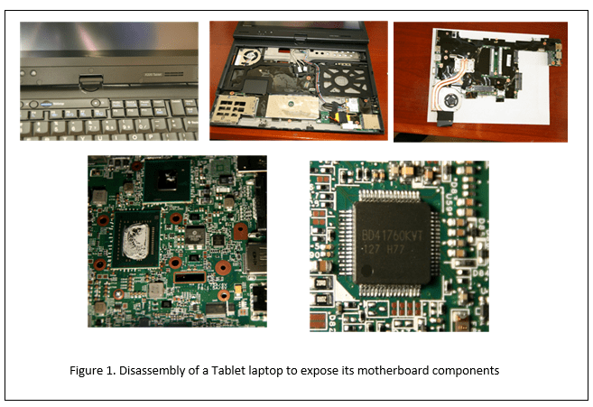
Not all hardware reverse engineering has to be very time-consuming and expensive. For example, in a patent infringement analysis case on the use of a patented invention in a particular laptop, it may be sufficient to simply disassemble the laptop to expose the motherboard and study the various integrated circuits (ICs) used on that mother board. In some cases, the datasheet publicly available on those ICs can provide the evidence on the use of the patented technology being used. In other cases, the source code used on those ICs may have to be analyzed to verify the infringement. Figure 1 shows one such disassembly for a Lenovo X220 Tablet laptop.
Hardware Reverse Engineering Tools
Of course, there are times when the claimed inventions in the infringement analysis case have to do with the circuits inside an IC and no public information about them is available. Similarly, the case may be that a legacy IC design has been acquired by a company but the circuit design documentation is missing. Whatever the case may be, design information about the circuitry inside the IC and how it operates is necessary and the only way to gain that information is by peering deep inside the chip.
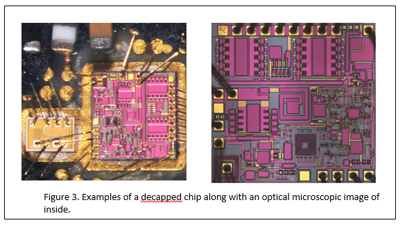
This is where sophisticated tools, laboratories and processes may have to be employed to achieve the goals. This is especially the case with today’s ever-decreasing geometry of ICs and increased number of gates (up to 100s of millions) per chip. In order to even reach the circuits of interest, first the packaging has to be removed. Usually (but not always), corrosive acids are used to etch off the packaging material without damaging the die inside.
Once the packaging is off, the delayering process starts. This involves layer by layer etching off the layers of the die under consideration to reach the layer of interest. Specialty labs maintain many different methods and solutions for various silicon processes to delayer the chips. Dealing with a reputable lab and knowing how to manage and monitor the quality of their work is important.
Advanced imaging laboratories can help in exposing the internal gates and interconnections of the chips, whether using optical, SEM (scanning electron microscopy), or TEM (transmission electron microscopy) imaging. A cross-sectional image may be used to gain insight into the layers of the chip, which could help with the delayering process as well. Advanced imaging laboratories can also play a crucial role in exposing the internal gates and interconnections of the chips, whether using optical, SEM (scanning electron microscopy), or TEM (transmission electron microscopy) imaging. A cross-sectional image may be used to gain insight into the layers of the chip, which could help with the delayering process as well.
Circuit extraction can be done manually for smaller projects (larger geometries with fewer gates on the die). However, for state-of-the-art ICs, the process is accomplished using a set of software tools that align the various images for each layer, align the composite image of each layer with those of the other layers, and then read and annotate all the gate and connection information from the images combined. This is, obviously, a very time-consuming and expensive process. It is also prone to human as well as machine (software) errors. Hence, monitoring the accuracy of the tools is critical.
Once annotations are complete, the circuit extraction and analysis process can be accomplished. This requires a high level of experience in the field to be able to put together not only the circuit diagrams, but also the overall circuit architecture. Many different analyses can be run at this stage, depending on what information is being sought after.
In conclusion, the process of extracting the IC circuits requires different sets of expertise, tools, and laboratories to achieve the required goals. Just like building a house, it is very important to select a trustworthy and capable project manager to manage the entire process, critique each step of the way, and keep focus on what is necessary to do. Otherwise, it is easily possible to run up a large bill for the entire process and still not achieve the desired result. The process can be time-consuming and expensive, but it is essential for understanding the design and functionality of proprietary ICs or for identifying potential security vulnerabilities.
Keep in tune with our news and insights page to view upcoming recent blog articles and technology papers.


