Target Products
Certain stacked memory ICs
Purpose
Quantitatively measure stress within the chips
Procedure
-
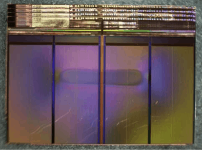
- A mult-die stacked chip was identified, decapsulated with hot acid after a cavity was ground into the top.
- The wirebonds were removed
- The die were separated from each other and from the substrate. Their thicknesses were measured.
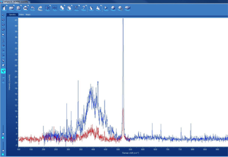
- A series of Raman measurements were made on the top surface of the exposed die. Several topological areas were used for the measurement. The Raman measurements give an indication of the overall stress.
- The die nitride passivation was then stripped to access the top metal layer. This metal layer was subsequently also removed to gain access to the interlayer dielectric. This layer is part of the overall metal-dielectric stack, and its stress level is generally representative of the stress in the entire stack.
- The Inter-Layer Dielectric (ILD) oxide was then removed and the series of Raman measurements were repeated to gain a quantitative understanding of the stress in the ILD.
- Measurement results were recorded and analyzed.
Result
- We successfully derived the stress level and its direction (compressive or tensile). The stress level was consistent with the die thinning used to stack the die into a package.


