Objective
Our primary goal was to study the power amplifier circuitry used in a cellular base station RF transceiver module and to determine its performance under various load conditions.
Approach
We performed a detailed circuit extraction in order to determine the microwave integrated circuit (MIC) topology of the PA module. Based on this circuit extraction, we performed a non-linear circuit simulation to accurately show load modulations.
Background
The power amplifier (PA) circuit is the last module of the transmitter chain before the duplexer circuit. It is well known to those with ordinary skills in the art that pre-driver and driver stages are commonly used in PA structures to raise the input power to sufficient levels required to drive the power (Main and Peaking) stages. The driver circuits often are designed as linear stages and do not play a role in efficiency enhancement.
In modern cellular network infrastructures such as the 3G and 4G standards, the modulated carrier signal shows a large amplitude excursion. Such signals are amplified to produce power levels of 20 to 80W using linear RF amplifier subsystems. One of the popular PA efficiency enhancement techniques is a combined circuit topology commonly known as the Doherty PA.
The Doherty amplifier is formed as a combination of two or more parallel power stages and their respective outputs are combined in a Doherty combiner. Each transistor is preceded by an input matching circuit and gate bias line and the output of each transistor is connected to a matching circuit and drain bias lines.
In a Doherty PA, the Main and peaking PAs operate in accord with the magnitude of the input signal. In lower input power levels (6-8dB below saturation) PA is active and the peaking amplifier remains off. This will result in enhancing the PA efficiency by lowering the peaking PA power dissipation. As the magnitude of the input signal increases, the main PA which is loaded by a resistive load twice its nominal value moves into a saturation state. This is a design parameter and is often set at around 6dB below the combined PA saturation level. Extending the saturation regime to lower input power levels is desirable as it improves the overall efficiency. This is before the peaking amplifier turns on and begins to contribute to the signal amplification.
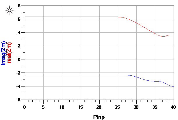
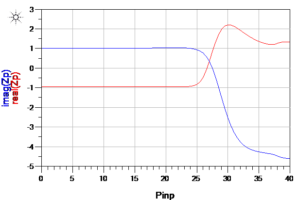
From this point onward, the impedance experienced by the main amplifier is reduced while the impedance of the peaking amplifier increases. In a Doherty amplifier circuit, as the peaking amplifier turns on, the load impedance experienced by the main amplifier decreases and the load impedance of the peaking amplifier increases gradually and in proportion to the amplitude of the input signal level. This is referred to as “Load Modulation”.
Circuit Extraction
The circuit extraction process involved accurately measuring the circuit dimensions and verifying the impedance and electrical values of passive circuit elements. The RF traces (controlled impedance) dimensions were measured by a specially-designed microscope. The surface-mount component values were removed from the circuit board and measured using LCR bridges.
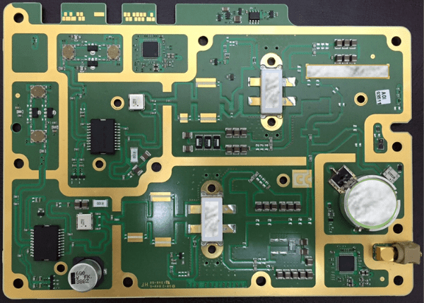
PA Module
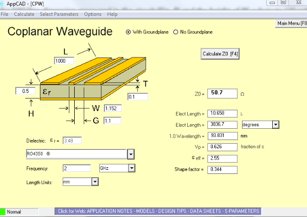
A further critical parameter was the extraction of the PCB substrate material properties. We used closed-form equations along with Avago software to determine the microstrip Substrate Dk. We also calculated the dielectric constant of the RF portion of multi-layer PCB. Based on these calculations, we found that these products are widely used in the RF industry and power amplifier products.
Dimension Measurement
Preliminary Nonlinear Circuit Simulation
Next, we attempted to simulate the circuit performance based on our circuit extraction results. We simulated a 100W device using the harmonic balance technique. The simulation results clearly indicated that load modulation took place as part of the PA’s functional performance.
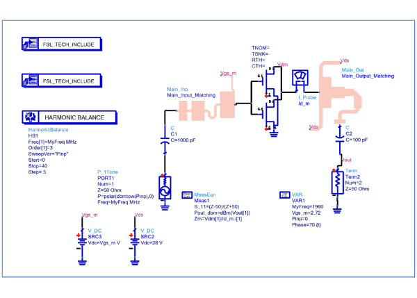
Main amplifier circuit simulation
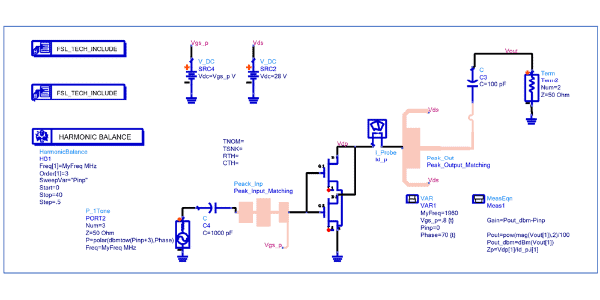
Peaking amplifier circuit simulation
Real and imaginary part of the Main amplifier impedance vs. PA input power, showing load modulation
Real and imaginary part of the Peaking amplifier impedance vs. PA input power, showing load modulation.
Conclusion
The power amplifier circuit under test was circuit extracted and simulated. The objectives of this exercise were met by definitively demonstrating that the amplifier circuit topology used in the product achieves its performance by load modulation.

