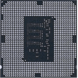
Target Product
A multicore processor
Purpose
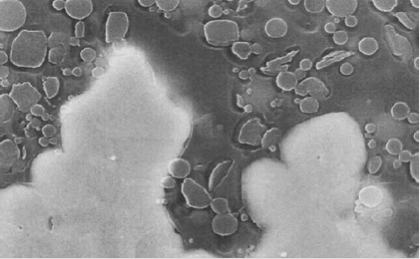
To analyze the interface between the copper layers and the insulator layers in the package PCB.
Procedure
- Decapped the chip
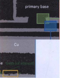
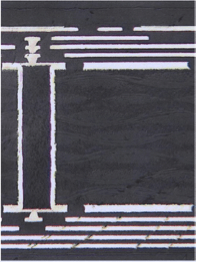
- Cross-sectioned the package PCB for SEM and TEM analysis
- TEM samples did not show the silica balls and resin clearly enough next to the copper (likely due to charging at the dielectric interface).
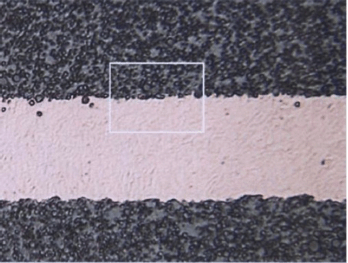
- Very high magnification SEM showed better resolution and significantly better contrast, especially after enhancing the copper with a very light etch.
- Measured
Result
Number of metal layers around the FR4 core was determined. The adhesion characteristics (including the shape and sizes of the silica particles and the holes) at the core and at subsequent metal layers were analyzed to determine the type of etching (chemical, physical bombardment, etc.) used at each layer.

